DRV8323/8353驱动
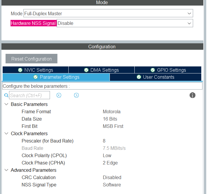
主要是将drv83xx对寄存器的操作封装成基于位域的结构体,这里我在SPI Interface Begin中将对SPI的操作、延时函数、系统时钟等封装成了接口和宏定义,根据自己的硬件进行对应修改即可使用;注意选用不同的drv83xx系列芯片时,需要在.h文件中修改成对应芯片型号的宏定义;SPI 配置为16bit 、FIRSTBIT_MSB 模式,时钟极性CPOL为LOW,CPHA为2EDGE,通讯
基于STM32G4(SPI接口)驱动DRV8353RS-CSDN博客
通讯配置:
SPI 配置为16bit 、FIRSTBIT_MSB 模式,时钟极性CPOL为LOW,CPHA为2EDGE,通讯速率小于10MHZ,同时片选引脚要设置为软件CS,我用硬件NSS会读不到数据;
寄存器配置:
DRV8323 的寄存器是易失(volatile)的——上电后寄存器会回到器件出厂/复位的默认值,不会永久保存你通过 SPI 写入的配置,因此每次上电都需要重新写入一次寄存器配置;
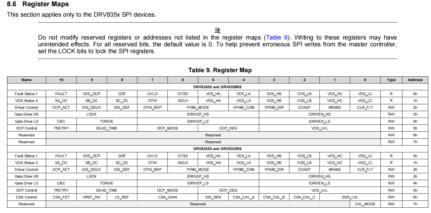
DRV8353寄存器:
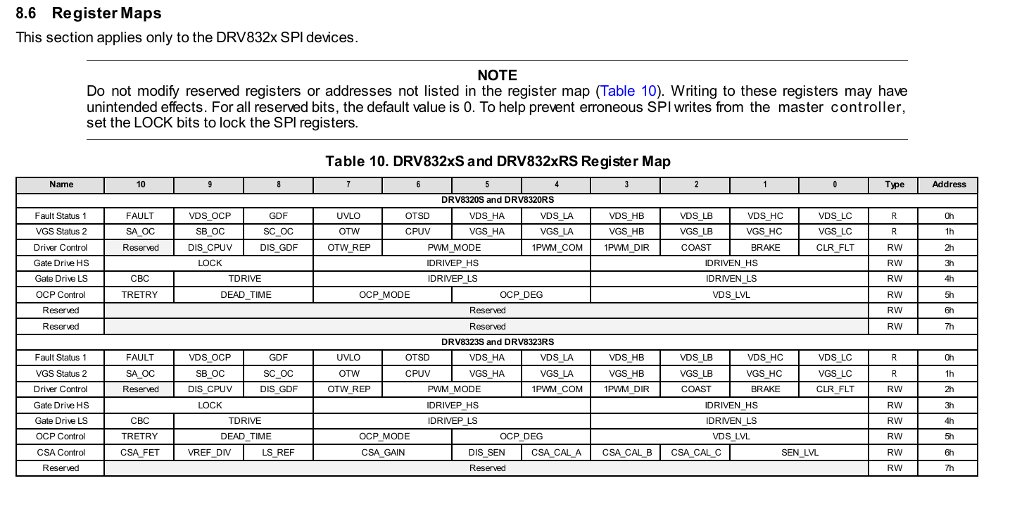
DRV8323寄存器:
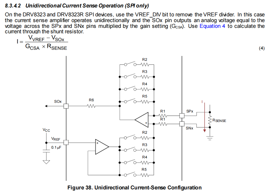
电流采样配置:
根据下面这个介绍,8323/8353电流采样公式为I = (Vref偏置电压 - VSOx采集到的电压)/(Gcsa放大倍数 * Rsense采样电阻阻值);需要注意的是一般我们认为流出电机电流为负电流,这里低侧相电阻采样从电阻上方流到地就是流出电机电流方向,因此在程序中我们采集的相电流数值还需要在上面电流采样公式得到的电流前加一个负号;
代码:
主要是将drv83xx对寄存器的操作封装成基于位域的结构体,这里我在SPI Interface Begin中将对SPI的操作、延时函数、系统时钟等封装成了接口和宏定义,根据自己的硬件进行对应修改即可使用;注意选用不同的drv83xx系列芯片时,需要在.h文件中修改成对应芯片型号的宏定义;
对DRV83xx系列寄存器的初始化操作在int DRV83XX_updateCfgPara(Stru_DRV83XX *stru_DRV83xxObj, StruDRV83XXCfgPara stru_config)中进行配置,如果初始化后还想在程序运行过程中执行其他操作类似自由滑行,可以调用下面的int DRV8323_COAST_enable(Stru_DRV83XX *stru_DRV83xxObj),如果想实现操作其他寄存器以自定义功能也可按照int DRV8323_COAST_enable(Stru_DRV83XX *stru_DRV83xxObj)函数的格式去编写;
代码链接:
DRV83XX驱动: DRV83XX系列 部分型号的SPI驱动 - Gitee.com
/* USER CODE BEGIN Header */
/**
 ******************************************************************************
 * File Name          :  drv_DRV835X.c
 * Description        :  DRV835X driver
 ******************************************************************************
 * @attention
 *
* COPYRIGHT:    Copyright (c) 2025
* CREATED BY:   Baseline
* DATE:         October 22th, 2025
 ******************************************************************************
 */
/* USER CODE END Header */
#include "drv83xx.h"
#include "drv83xx_reg.h"


/***********************************   SPI Interface Begin *********************************/
/* Private macro -------------------------------------------------------------*/
extern SPI_HandleTypeDef        hspi2;

/* Private define ------------------------------------------------------------*/
#define DEBUG
#define DEBUG_OUT(fmt, ...)   //printf("[DEBUG] " fmt "\n", ##__VA_ARGS__)

#define TIME_OUT                10
#define DEFAULT_GAIN            10
#define SYSCLK  120000000
#define Drv83xx_Commu_delayus   50     //The interval us between two communications

// DRV8353 SPI CS PIN
#define DRV835X_CS_EN           HAL_GPIO_WritePin(GPIOB,GPIO_PIN_12,GPIO_PIN_RESET)
#define DRV835X_CS_DIS          HAL_GPIO_WritePin(GPIOB,GPIO_PIN_12,GPIO_PIN_SET)

// DRV8353 ENABLE PIN
/*
    Gate driver enable. When this pin is logic low the device goes to a low power sleep mode.
    An 8 to 40-µs low pulse can be used to reset fault conditions.
*/
#define DRV835X_ENABLE_LOW      HAL_GPIO_WritePin(DRV8323_EN_GPIO_Port,DRV8323_EN_Pin,GPIO_PIN_RESET)
#define DRV835X_ENABLE_HIGH     HAL_GPIO_WritePin(DRV8323_EN_GPIO_Port,DRV8323_EN_Pin,GPIO_PIN_SET)


static int spi_transmit(uint16_t data) {
  int status;
	uint16_t data_response;
  //status = HAL_SPI_Transmit(&hspi2, (uint8_t *)&data, 1, TIME_OUT);  //16-bit Mode
	HAL_SPI_TransmitReceive(&hspi2, (uint8_t*)&data, (uint8_t*)&data_response, 1, HAL_MAX_DELAY);
  return status;
}

static int spi_receive(uint16_t data, uint16_t *data_response) {
  int status;
  //status = HAL_SPI_Receive(&hspi2, (uint8_t *)&data, 1, TIME_OUT);   //16-bit Mode
	HAL_SPI_TransmitReceive(&hspi2, (uint8_t*)&data, (uint8_t*)data_response, 1, HAL_MAX_DELAY);
  return status;
}

static void Delay_ms(int ms)
{
	HAL_Delay(ms);
}


static void Delay_us(int _us)
{
	 uint32_t ticks;
    uint32_t told, tnow, tcnt = 0;

    // 计算需要的时钟数 = 延迟微秒数 * 每微秒的时钟数
    ticks = _us * (SYSCLK / 1000000);

    // 获取当前的SysTick值
    told = SysTick->VAL;

    while (1)
    {
        // 重复刷新获取当前的SysTick值
        tnow = SysTick->VAL;

        if (tnow != told)
        {
            if (tnow < told)
                tcnt += told - tnow;
            else
                tcnt += SysTick->LOAD - tnow + told;

            told = tnow;

            // 如果达到了需要的时钟数,就退出循环
            if (tcnt >= ticks)
                break;
        }
    }
}
/***********************************   SPI Interface End *********************************/


/* Private variables ---------------------------------------------------------*/
Stru_DRV83XX stru_DRV8323Obj;

StruDRV83XXCfgPara stru_config =
{
    // Driver Control Register (address = 0x02h)
   .PWM_MODE = PWM_MODE_3X,


   //Gate Drive HS Register (address = 0x03h)
   .IDRIVEP_HS = IDRIVEP_HS_1000MA,
   .IDRIVEN_HS = IDRIVEN_HS_2000MA,
   .LOCK = LOCK_OFF,

   // Gate Drive LS Register (address = 0x04h)
   .IDRIVEN_LS = IDRIVEN_LS_2000MA,
   .IDRIVEP_LS = IDRIVEP_LS_1000MA,
   .TDRIVE = TDRIVE_4000NS,
   .CBC = PWM_GIVER_ENABLE,  // 1b = For VDS_OCP and SEN_OCP, the fault is cleared when
                             // a new PWM input is given or after tRETRY

    // OCP Control Register (address = 0x05h)
   .VDS_LVL =  VDS_OCP_LVL_0_94,
   .OCP_DEG =  OCP_DEG_6US,
   .OCP_MODE = OCP_Mode_REPORT,
   .DEAD_TIME = DEADTIME_400NS,

    // CSA Control Register (DRV8353 and DRV8353R Only) (address = 0x06h)
#ifdef HAS_CSA_Control_Fields
   .SEN_LVL = SEN_OCP_LVL_0_25,   //  00b = Sense OCP 0.25 V
   .CSA_GAIN = CSA_GAIN_40,   //  03b = 40-V/V shunt amplifier gain
   .VREF_DIV = VREF_DIV_2,    //  1b = Sense amplifier reference voltage is VREF divided by 2
	 .CSA_CAL_A = CSA_CAL_A_DIS,
	 .CSA_CAL_B = CSA_CAL_B_DIS,
	 .CSA_CAL_C = CSA_CAL_C_DIS,

#endif
};

/* Private function prototypes -----------------------------------------------*/
static uint16_t read_reg(uint16_t address);
static int write_reg(uint16_t address, uint16_t data);

void DRV83XX_Init( void )
{
    DRV835X_ENABLE_LOW;
    Delay_ms(10);
    DRV835X_ENABLE_HIGH;
    Delay_ms(10);

    if(0 != DRV83XX_updateCfgPara(&stru_DRV8323Obj, stru_config))
		{
#ifdef DEBUG
			DEBUG_OUT("DRV83XX write reg failed\n");
#endif
		}
	  Delay_ms(100);
		DRV83XX_read_ALLReg(&stru_DRV8323Obj);

}


int DRV83XX_updateCfgPara(Stru_DRV83XX *stru_DRV83xxObj, StruDRV83XXCfgPara stru_config)
{
    int Status;
    uint16_t data;
    // Driver Control Register (address = 0x02h)
    stru_DRV83xxObj->drvCtrl_obj.ctrlRegObj.PWM_MODE  = stru_config.PWM_MODE;
    data = stru_DRV83xxObj->drvCtrl_obj.data;
    Status = Status | write_reg( DCR, data);

    //Gate Drive HS Register (address = 0x03h)
    stru_DRV83xxObj->drvGateHS_obj.gateHSRegObj.IDRIVEP_HS = stru_config.IDRIVEP_HS;
    stru_DRV83xxObj->drvGateHS_obj.gateHSRegObj.IDRIVEN_HS = stru_config.IDRIVEN_HS;
    stru_DRV83xxObj->drvGateHS_obj.gateHSRegObj.LOCK = stru_config.LOCK;
    data = stru_DRV83xxObj->drvGateHS_obj.data;
    Status = Status | write_reg( HSR, data);

    // Gate Drive LS Register (address = 0x04h)
    stru_DRV83xxObj->drvGateLS_obj.gateLSRegObj.IDRIVEN_LS = stru_config.IDRIVEN_LS;
    stru_DRV83xxObj->drvGateLS_obj.gateLSRegObj.IDRIVEP_LS = stru_config.IDRIVEP_LS;
    stru_DRV83xxObj->drvGateLS_obj.gateLSRegObj.TDRIVE = stru_config.TDRIVE;
    stru_DRV83xxObj->drvGateLS_obj.gateLSRegObj.CBC = stru_config.CBC;
    data = stru_DRV83xxObj->drvGateLS_obj.data;
    Status = Status | write_reg( LSR, data);

    // OCP Control Register (address = 0x05h)
    stru_DRV83xxObj->drvOcp_obj.ocpObj.VDS_LVL =  stru_config.VDS_LVL;
    stru_DRV83xxObj->drvOcp_obj.ocpObj.OCP_DEG =  stru_config.OCP_DEG;
    stru_DRV83xxObj->drvOcp_obj.ocpObj.OCP_MODE = stru_config.OCP_MODE;
    stru_DRV83xxObj->drvOcp_obj.ocpObj.DEAD_TIME = stru_config.DEAD_TIME;
    data = stru_DRV83xxObj->drvOcp_obj.data;
    Status = Status | write_reg( OCPCR, data);


	    // CSA Control Register (DRV8353 and DRV8353R Only) (address = 0x06h)
#ifdef HAS_CSA_Control_Fields
    stru_DRV83xxObj->drvCsa_obj.csaObj.SEN_LVL  = stru_config.SEN_LVL;
    stru_DRV83xxObj->drvCsa_obj.csaObj.CSA_GAIN = stru_config.CSA_GAIN;
    stru_DRV83xxObj->drvCsa_obj.csaObj.VREF_DIV = stru_config.VREF_DIV;
		stru_DRV83xxObj->drvCsa_obj.csaObj.CSA_CAL_A = stru_config.CSA_CAL_A;
		stru_DRV83xxObj->drvCsa_obj.csaObj.CSA_CAL_B = stru_config.CSA_CAL_B;
		stru_DRV83xxObj->drvCsa_obj.csaObj.CSA_CAL_C = stru_config.CSA_CAL_C;
		data = stru_DRV83xxObj->drvCsa_obj.data;
    Status = Status | write_reg( CSACR, data);
#endif

    return Status;
}

static uint16_t read_reg(uint16_t address)
{
	  uint16_t data, data_response;
    Input_WrReg stru_Input_WrRegObj;
    stru_Input_WrRegObj.inputRegObj.WR =  R_MODE;
    stru_Input_WrRegObj.inputRegObj.ADDRESS = address;
    data = stru_Input_WrRegObj.data;

    DRV835X_CS_EN;
	  spi_receive(data, &data_response);
    DRV835X_CS_DIS;
    Delay_us(Drv83xx_Commu_delayus);

    return (data_response & 0x7FF);
}


static int write_reg(uint16_t address, uint16_t data)
{
    Input_WrReg stru_Input_WrRegObj;
    uint16_t data_response;
    stru_Input_WrRegObj.inputRegObj.WR =  W_MODE;
    stru_Input_WrRegObj.inputRegObj.ADDRESS = address;
    stru_Input_WrRegObj.inputRegObj.DATA = data;
    data = stru_Input_WrRegObj.data;

		DRV835X_CS_EN;
		spi_transmit(data);
		DRV835X_CS_DIS;
		Delay_us(Drv83xx_Commu_delayus);
	  data_response = read_reg(address);
		if(data_response != (data & 0x7FF))
		{
			 return -1;
		}

    return 0;
}


void DRV83XX_read_ALLReg(Stru_DRV83XX *stru_DRV83xxObj)
{
	  stru_DRV83xxObj->faultStatusReg1_obj.data = read_reg( FSR1 );
    stru_DRV83xxObj->faultStatusReg2_obj.data = read_reg( FSR2 );

    stru_DRV83xxObj->drvCtrl_obj.data = read_reg( DCR );
	  stru_DRV83xxObj->drvGateHS_obj.data = read_reg( HSR );
    stru_DRV83xxObj->drvGateLS_obj.data = read_reg( LSR );

    stru_DRV83xxObj->drvOcp_obj.data = read_reg( OCPCR );
    stru_DRV83xxObj->drvCsa_obj.data = read_reg( CSACR );
    stru_DRV83xxObj->drvCfg_obj.data = read_reg( DFGCR );
}

void DRV83XX_read_FaultStatusReg1(Stru_DRV83XX *stru_DRV83xxObj)
{
    stru_DRV83xxObj -> faultStatusReg1_obj .data = read_reg( FSR1 );
}

void DRV83XX_read_FaultStatusReg2(Stru_DRV83XX *stru_DRV83xxObj)
{
    stru_DRV83xxObj -> faultStatusReg2_obj.data = read_reg( FSR2 );
}

int DRV8323_COAST_Disable(Stru_DRV83XX *stru_DRV83xxObj)
{
		stru_DRV83xxObj->drvCtrl_obj.data = read_reg(DCR);
	  stru_DRV83xxObj->drvCtrl_obj.ctrlRegObj.COAST  = COAST_DIS;
    return write_reg(DCR, stru_DRV83xxObj->drvCtrl_obj.data);
}

int DRV8323_COAST_enable(Stru_DRV83XX *stru_DRV83xxObj)
{
	  stru_DRV83xxObj->drvCtrl_obj.data = read_reg(DCR);
	  stru_DRV83xxObj->drvCtrl_obj.ctrlRegObj.COAST  = COAST_EN;
    return write_reg(DCR, stru_DRV83xxObj->drvCtrl_obj.data);
}

int DRV8323_CurrentCAL_enable(Stru_DRV83XX *stru_DRV83xxObj)
{
		stru_DRV83xxObj->drvCsa_obj.data = read_reg(CSACR);
		stru_DRV83xxObj->drvCsa_obj.csaObj.CSA_CAL_A = CSA_CAL_A_EN;
		stru_DRV83xxObj->drvCsa_obj.csaObj.CSA_CAL_B = CSA_CAL_B_EN;
		stru_DRV83xxObj->drvCsa_obj.csaObj.CSA_CAL_C = CSA_CAL_C_EN;
    return write_reg(DCR, stru_DRV83xxObj->drvCtrl_obj.data);
}

int DRV8323_CurrentCAL_disable(Stru_DRV83XX *stru_DRV83xxObj)
{
		stru_DRV83xxObj->drvCsa_obj.data = read_reg(CSACR);
		stru_DRV83xxObj->drvCsa_obj.csaObj.CSA_CAL_A = CSA_CAL_A_DIS;
		stru_DRV83xxObj->drvCsa_obj.csaObj.CSA_CAL_B = CSA_CAL_B_DIS;
		stru_DRV83xxObj->drvCsa_obj.csaObj.CSA_CAL_C = CSA_CAL_C_DIS;
		return write_reg(DCR, stru_DRV83xxObj->drvCtrl_obj.data);
}

/* End of this file */
在.h芯片中旋转使用的DRV83xx系列具体芯片型号
/* USER CODE BEGIN Header */
/**
 ******************************************************************************
 * File Name          :  drv_DRV835X.c
 * Description        :  DRV835X driver
 ******************************************************************************
 * @attention
 *
* COPYRIGHT:    Copyright (c) 2025
* CREATED BY:   Baseline
* DATE:         October 22th, 2025
 ******************************************************************************
 */
/* USER CODE END Header */

/* Includes ------------------------------------------------------------------*/
#ifndef DRV835X_H
#define DRV835X_H

#ifdef _cplusplus
extern "C"
{
#endif

#include "main.h"
#include <stdio.h>

/* --- Check whether the user has specified a model --- */
//#define DRV8350
//#define DRV8353
//#define DRV8320
#define DRV8323      //Must : Select your Specifically DRV83xx Chip

#if !defined(DRV8350) && !defined(DRV8353) && !defined(DRV8320) && !defined(DRV8323)
  #error "Please define a driver model macro (e.g. -DDRIVER_DRV8353A) in build options"
#endif

/* --- Map model types to feature macros --- */
/* For models with OCP_ACT / DIS_GDUV */
#if defined(DRV8350) || defined(DRV8353)
  #define HAS_OCP_ACT    1
  #define HAS_DIS_GDUV   1
	#define HAS_DRV835X_VDS_LVL  1
#endif

/* For models with DIS_CPUV */
#if defined(DRV8320) || defined(DRV8323)
  #define HAS_DIS_CPUV   1
	#define HAS_DRV832X_VDS_LVL  1
#endif

#if defined(DRV8323) || defined(DRV8353)
  #define HAS_CSA_Control_Fields 1
#endif

#if defined(DRV8353)
  #define HAS_CAL_MODE   1
#endif
/* --- Check whether the user has specified a model End--- */


#if defined ( __CC_ARM   )
#pragma anon_unions
#endif

#define  W_MODE              0
#define  R_MODE              1

/**************************************************************/
/*
    INPUT data structure
*/
typedef struct
{
    uint16_t DATA      : 11;    // 11 data bits, D (bits B11 through B0)
    uint16_t ADDRESS   : 4;     // 4 address bits, A (bits B14 through B11)

    uint16_t WR        : 1;     // 1 read or write bit, W (bit B15)
}Input_WrReg_bit;

typedef struct
{
   union
   {
      uint16_t data;
      Input_WrReg_bit inputRegObj;
   };
} Input_WrReg ;

/*
    Fault Status Register 1 (address = 0x00h)
*/
typedef struct
{
    uint16_t VDS_LC    : 1;
    uint16_t VDS_HC    : 1;
    uint16_t VDS_LB    : 1;
    uint16_t VDS_HB    : 1;

    uint16_t VDS_LA    : 1;
    uint16_t VDS_HA    : 1;
    uint16_t OTSD      : 1;
    uint16_t UVLO      : 1;

    uint16_t GDF       : 1;
    uint16_t VDS_OCP   : 1;
    uint16_t FAULT     : 1;

    uint16_t res       : 5;

}Fault_StatusReg1_bit;

typedef struct
{
   union
   {
      uint16_t data;
      Fault_StatusReg1_bit fault1RegObj;
   };
} Fault_StatusReg1 ;

/*
    Fault Status Register 2 (address = 0x01h)
*/
typedef struct
{
    uint16_t VGS_LC    : 1;
    uint16_t VGS_HC    : 1;

    uint16_t VGS_LB    : 1;
    uint16_t VGS_HB    : 1;

    uint16_t VDS_LA    : 1;
    uint16_t VDS_HA    : 1;

    uint16_t GDUV      : 1;
    uint16_t OTW       : 1;

    uint16_t SC_OC     : 1;
    uint16_t SB_OC     : 1;
    uint16_t SA_OC     : 1;

    uint16_t res       : 5;

}Fault_StatusReg2_bit;

typedef struct
{
   union
   {
      uint16_t data;
      Fault_StatusReg2_bit fault2RegObj;
   };
} Fault_StatusReg2;

/*
    Driver Control Register (address = 0x02h)
*/
typedef struct
{
    uint16_t CLR_FLT  : 1;
    uint16_t BRAKE    : 1;
    uint16_t COAST    : 1;
    uint16_t PWM1_DIR : 1;

    uint16_t PWM1_COM : 1;
    uint16_t PWM_MODE : 2;
    uint16_t OTW_REP  : 1;

    uint16_t DIS_GDF  : 1;

#ifdef  HAS_DIS_GDUV
    uint16_t DIS_GDUV : 1;
#elif   HAS_DIS_CPUV
	  uint16_t DIS_CPUV : 1;
#else
	  uint16_t bit9_RESERVE : 1;
#endif

#ifdef  HAS_OCP_ACT
    uint16_t OCP_ACT  : 1;
#else
    uint16_t bit10_RESERVE : 1;
#endif

    uint16_t res      : 5;

}Drv_CtrlReg_bit;

typedef struct
{
   union
   {
      uint16_t data;
      Drv_CtrlReg_bit ctrlRegObj;
   };
} Drv_CtrlReg ;

/*
    Gate Drive HS Register (address = 0x03h)
*/
typedef struct
{
    uint16_t IDRIVEN_HS  : 4;
    uint16_t IDRIVEP_HS  : 4;

    uint16_t LOCK        : 3;
    uint16_t res         : 5;

}Drv_GateHS_bit;

typedef struct
{
   union
   {
      uint16_t data;
      Drv_GateHS_bit gateHSRegObj;
   };
} Drv_GateHS;


/*
    Gate Drive LS Register (address = 0x04h)
*/
typedef struct
{
    uint16_t IDRIVEN_LS  : 4;
    uint16_t IDRIVEP_LS  : 4;

    uint16_t TDRIVE      : 2;
    uint16_t CBC         : 1;

    uint16_t res         : 5;

}Drv_GateLS_bit;

typedef struct
{
   union
   {
      uint16_t data;
      Drv_GateLS_bit gateLSRegObj;
   };
} Drv_GateLS;

/*
    OCP Control Register (address = 0x05h)
*/
typedef struct
{
    uint16_t VDS_LVL     : 4;
    uint16_t OCP_DEG     : 2;

    uint16_t OCP_MODE    : 2;
    uint16_t DEAD_TIME   : 2;

    uint16_t TRETRY      : 1;

    uint16_t res         : 5;

}Drv_OCP_bit;

typedef struct
{
   union
   {
      uint16_t data;
      Drv_OCP_bit ocpObj;
   };
} Drv_OCP;

/*
    CSA Control Register (DRV8353 and DRV8353R Only) (address = 0x06h)
*/
typedef struct
{
#ifdef HAS_CSA_Control_Fields
    uint16_t SEN_LVL     : 2;

    uint16_t CSA_CAL_C   : 1;
    uint16_t CSA_CAL_B   : 1;
    uint16_t CSA_CAL_A   : 1;
    uint16_t DIS_SEN     : 1;

    uint16_t CSA_GAIN    : 2;
    uint16_t LS_REF      : 1;
    uint16_t VREF_DIV    : 1;

    uint16_t CSA_FET     : 1;
#else
	  uint16_t bit0_10_RESERVE : 11;
#endif
    uint16_t res         : 5;
}Drv_CSA_bit;

typedef struct
{
   union
   {
      uint16_t data;
      Drv_CSA_bit csaObj;
   };
} Drv_CSA;

/*
    Driver Configuration Register (DRV8353 and DRV8353R Only) (address = 0x07h)
*/
typedef struct
{
#if HAS_CAL_MODE
    uint16_t SEN_LVL        : 1;
#else
	  uint16_t bit0_RESERVE   : 1;
#endif
    uint16_t bit1_10_RESERVE     : 10;
    uint16_t res         : 5;

}Drv_Cfg_bit;

typedef struct
{
   union
   {
      uint16_t data;
      Drv_Cfg_bit cfgObj;
   };
} Drv_Cfg;

/**************************************************************/
typedef struct
{
    Fault_StatusReg1  faultStatusReg1_obj;
    Fault_StatusReg2  faultStatusReg2_obj;

	  Drv_CtrlReg drvCtrl_obj;
    Drv_GateLS drvGateLS_obj;
    Drv_GateHS drvGateHS_obj;

    Drv_OCP drvOcp_obj;
	  Drv_CSA drvCsa_obj;
	  Drv_Cfg drvCfg_obj;
}Stru_DRV83XX;
extern Stru_DRV83XX stru_DRV8323Obj;


typedef struct
{
   // Driver Control Register (address = 0x02h)
   uint8_t PWM_MODE;


   //Gate Drive HS Register (address = 0x03h)
   uint8_t IDRIVEP_HS;
   uint8_t IDRIVEN_HS;
   uint8_t LOCK;

   // Gate Drive LS Register (address = 0x04h)
   uint8_t IDRIVEN_LS;
   uint8_t IDRIVEP_LS;
   uint8_t TDRIVE;
   uint8_t CBC;

   // OCP Control Register (address = 0x05h)
   uint8_t VDS_LVL;
   uint8_t OCP_DEG;
   uint8_t OCP_MODE;
   uint8_t DEAD_TIME;

   // CSA Control Register (DRV8353 and DRV8353R Only) (address = 0x06h)
   uint8_t SEN_LVL;
   uint8_t CSA_GAIN;
   uint8_t VREF_DIV;
   uint8_t CSA_CAL_A;
	 uint8_t CSA_CAL_B;
   uint8_t CSA_CAL_C;
} StruDRV83XXCfgPara;


void DRV83XX_Init(void);
int DRV83XX_updateCfgPara(Stru_DRV83XX *stru_DRV83xxObj, StruDRV83XXCfgPara stru_config);

void DRV83XX_read_ALLReg(Stru_DRV83XX *stru_DRV83xxObj);
void DRV83XX_read_FaultStatusReg1(Stru_DRV83XX *stru_DRV83xxObj);
void DRV83XX_read_FaultStatusReg2(Stru_DRV83XX *stru_DRV83xxObj);
int DRV8323_COAST_Disable(Stru_DRV83XX *stru_DRV83xxObj);
int DRV8323_COAST_enable(Stru_DRV83XX *stru_DRV83xxObj);
int DRV8323_CurrentCAL_enable(Stru_DRV83XX *stru_DRV83xxObj);
int DRV8323_CurrentCAL_disable(Stru_DRV83XX *stru_DRV83xxObj);

#ifdef _cplusplus
}
#endif


#endif  /* DRV835X_H */
/* USER CODE BEGIN Header */
/**
 ******************************************************************************
 * File Name          :  drv_DRV835X.c
 * Description        :  DRV835X driver
 ******************************************************************************
 * @attention
 *
* COPYRIGHT:    Copyright (c) 2025
* CREATED BY:   Baseline
* DATE:         October 22th, 2025
 ******************************************************************************
 */
/* USER CODE END Header */

/* Includes ------------------------------------------------------------------*/
#ifndef __DRV_DRV83XX_REG_H
#define __DRV_DRV83XX_REG_H

#ifdef _cplusplus
extern "C"
{
#endif

#include "main.h"
#include "drv83xx.h"


/// ****************** Registers ******************///
#define FSR1             0x0     /// Fault Status Register 1   --  only read
#define FSR2             0x1     /// Fault Status Register 2   --  only read
#define DCR              0x2     /// Drive Control Register    --  read and write
#define HSR              0x3     /// Gate Drive HS Register    --  read and write
#define LSR              0x4     /// Gate Drive LS Register    --  read and write
#define OCPCR            0x5     /// OCP Control Register      --  read and write
#define CSACR            0x6     /// CSA Control Register      --  read and write
#define DFGCR            0x7     /// Driver Configuration Register   --  read and write

/// ****** Drive Control Fields ******///(address = 0x02h)
#ifdef HAS_OCP_ACT
	#define OCP_ACT_Associated  0x0     //Associated half-bridge is shutdown in response to  VDS_OCP and SEN_OCP
	#define OCP_ACT_Global      0x1     //All three half-bridges are shutdown in response to VDS_OCP and SEN_OCP
#endif
#ifdef  HAS_DIS_GDUV
	#define DIS_GDUV_EN         0x0     ///VCP and VGLS undervoltage lockout fault is enabled
	#define DIS_GDUV_DIS        0x1
#endif

#ifdef HAS_DIS_CPUV
	#define DIS_CPUV_EN         0x0     /// Charge pump UVLO fault
	#define DIS_CPUV_DIS        0x1
#endif

#define DIS_GDF_EN          0x0     /// Gate drive fault
#define DIS_GDF_DIS         0x1
#define OTW_REP_DIS         0x0
#define OTW_REP_EN          0x1     /// Over temp warning reported on nFAULT/FAULT bit

#define PWM_MODE_6X         0x0     /// PWM Input Modes  Chip not allow Upper and lower pipes straight through
#define PWM_MODE_3X         0x1     /// 3X INHx PWM Control,in this mode all INLx should be High level
#define PWM_MODE_1X         0x2     /// Typically used for six-position reversing control
#define PWM_MODE_IND        0x3     /// 6X PWM but Chip allow Upper and lower pipes straight through

#define PWM_1X_COM_SYNC     0x0     /// 1x PWM Mode synchronou rectification
#define PWM_1X_COM_ASYNC    0x1

#define PWM_1X_DIR_0        0x0     /// In 1x PWM mode this bit is ORed with the INHC (DIR) input
#define PWM_1X_DIR_1        0x1

#define COAST_DIS           0x0
#define COAST_EN            0x1      ///put all MOSFETs in the Hi-Z state, Allow the motor to coast freely

#define BRAKE_DIS           0x0
#define BRAKE_EN            0x1      ///turn on all three low-side MOSFETs, Apply short-circuit braking to the motor

#define CLR_FLT_DIS         0x0
#define CLR_FLT__EN         0x1      ///clear latched fault bits.This bit automatically resets after being writen


/// ****** Gate Drive HS Fields ******///(address = 0x03h)
#define LOCK_ON             0x6    //Lock all register write operations except for specific registers (such as bits [0–2] at address 0x02).
#define LOCK_OFF            0x3    //Unlocked state enabled; all writable registers can now be modified.

#define IDRIVEP_HS_10MA     0x0     /// Gate drive high side turn on current
#define IDRIVEP_HS_30MA     0x1
#define IDRIVEP_HS_60MA     0x2
#define IDRIVEP_HS_80MA     0x3
#define IDRIVEP_HS_120MA    0x4
#define IDRIVEP_HS_140MA    0x5
#define IDRIVEP_HS_170MA    0x6
#define IDRIVEP_HS_190MA    0x7
#define IDRIVEP_HS_260MA    0x8
#define IDRIVEP_HS_330MA    0x9
#define IDRIVEP_HS_370MA    0xA
#define IDRIVEP_HS_440MA    0xB
#define IDRIVEP_HS_570MA    0xC
#define IDRIVEP_HS_680MA    0xD
#define IDRIVEP_HS_820MA    0xE
#define IDRIVEP_HS_1000MA   0xF     /// Default :

#define IDRIVEN_HS_20MA     0x0     /// High side turn off current
#define IDRIVEN_HS_60MA     0x1
#define IDRIVEN_HS_120MA    0x2
#define IDRIVEN_HS_160MA    0x3
#define IDRIVEN_HS_240MA    0x4
#define IDRIVEN_HS_280MA    0x5
#define IDRIVEN_HS_340MA    0x6
#define IDRIVEN_HS_380MA    0x7
#define IDRIVEN_HS_520MA    0x8
#define IDRIVEN_HS_660MA    0x9
#define IDRIVEN_HS_740MA    0xA
#define IDRIVEN_HS_880MA    0xB
#define IDRIVEN_HS_1140MA   0xC
#define IDRIVEN_HS_1360MA   0xD
#define IDRIVEN_HS_1640MA   0xE
#define IDRIVEN_HS_2000MA   0xF    /// Default :

/// ****** Gate Drive LS Fields ****** /// (address = 0x04h)

                                 //PWM_GIVER_ENABLE/DISABLE Active only when OCP_MODE = 01b
#define  PWM_GIVER_DISABLE  0x0  //Overcurrent faults will automatically clear after a fixed delay of tRETRY .
#define  PWM_GIVER_ENABLE   0x1  /// Default :the fault is cleared when a new PWM input is given or after tRETRY

#define TDRIVE_500NS        0x0     /// Peak gate-current drive time
#define TDRIVE_1000NS       0x1
#define TDRIVE_2000NS       0x2
#define TDRIVE_4000NS       0x3     /// Default :

#define IDRIVEP_LS_10MA     0x0     /// Gate drive high side turn on current
#define IDRIVEP_LS_30MA     0x1
#define IDRIVEP_LS_60MA     0x2
#define IDRIVEP_LS_80MA     0x3
#define IDRIVEP_LS_120MA    0x4
#define IDRIVEP_LS_140MA    0x5
#define IDRIVEP_LS_170MA    0x6
#define IDRIVEP_LS_190MA    0x7
#define IDRIVEP_LS_260MA    0x8
#define IDRIVEP_LS_330MA    0x9
#define IDRIVEP_LS_370MA    0xA
#define IDRIVEP_LS_440MA    0xB
#define IDRIVEP_LS_570MA    0xC
#define IDRIVEP_LS_680MA    0xD
#define IDRIVEP_LS_820MA    0xE
#define IDRIVEP_LS_1000MA   0xF     /// Default :

#define IDRIVEN_LS_20MA     0x0     /// High side turn off current
#define IDRIVEN_LS_60MA     0x1
#define IDRIVEN_LS_120MA    0x2
#define IDRIVEN_LS_160MA    0x3
#define IDRIVEN_LS_240MA    0x4
#define IDRIVEN_LS_280MA    0x5
#define IDRIVEN_LS_340MA    0x6
#define IDRIVEN_LS_380MA    0x7
#define IDRIVEN_LS_520MA    0x8
#define IDRIVEN_LS_660MA    0x9
#define IDRIVEN_LS_740MA    0xA
#define IDRIVEN_LS_880MA    0xB
#define IDRIVEN_LS_1140MA   0xC
#define IDRIVEN_LS_1360MA   0xD
#define IDRIVEN_LS_1640MA   0xE
#define IDRIVEN_LS_2000MA   0xF    /// Default :


/// ****** OCP Control Fields ******///  (address = 0x05h)
#define TRETRY_4MS          0x0     /// VDS OCP and SEN OCP retry time
#define TRETRY_50US         0x1

#define DEADTIME_50NS       0x0     /// Deadtime
#define DEADTIME_100NS      0x1     /// Default :
#define DEADTIME_200NS      0x2
#define DEADTIME_400NS      0x3


#define OCP_Mode_LATCH           0x0     ///Overcurrent causes a latched fault
#define OCP_Mode_RETRY           0x1     ///Default :Overcurrent causes an automatic retrying fault
#define OCP_Mode_REPORT          0x2     ///Overcurrent is report only but no action is taken
#define OCP_Mode_NONE            0x3     ///Overcurrent is not reported and no action is taken

#define OCP_DEG_2US         0x0     /// OCP Deglitch Time
#define OCP_DEG_4US         0x1     /// Default :
#define OCP_DEG_6US         0x2
#define OCP_DEG_8US         0x3


#ifdef HAS_DRV832X_VDS_LVL  //VDS_LVL :MOSFET Drain-Source Voltage OverCurrent Protect Detection Threshold
	#define VDS_OCP_LVL_0_06        0x0
	#define VDS_OCP_LVL_0_13        0x1
	#define VDS_OCP_LVL_0_2         0x2
	#define VDS_OCP_LVL_0_26        0x3
	#define VDS_OCP_LVL_0_31        0x4
	#define VDS_OCP_LVL_0_45        0x5
	#define VDS_OCP_LVL_0_53        0x6
	#define VDS_OCP_LVL_0_6         0x7
	#define VDS_OCP_LVL_0_68        0x8
	#define VDS_OCP_LVL_0_75        0x9     //Default : VDS_OCP_LVL = 0.75 V
	#define VDS_OCP_LVL_0_94        0xA
	#define VDS_OCP_LVL_1_13        0xB
	#define VDS_OCP_LVL_1_3         0xC
	#define VDS_OCP_LVL_1_5         0xD
	#define VDS_OCP_LVL_1_7         0xE
	#define VDS_OCP_LVL_1_88        0xF
#endif

#ifdef HAS_DRV835X_VDS_LVL
	#define VDS_OCP_LVL_0_06        0x0
	#define VDS_OCP_LVL_0_07        0x1
	#define VDS_OCP_LVL_0_08        0x2
	#define VDS_OCP_LVL_0_09        0x3
	#define VDS_OCP_LVL_0_1         0x4
	#define VDS_OCP_LVL_0_2         0x5
	#define VDS_OCP_LVL_0_3         0x6
	#define VDS_OCP_LVL_0_4         0x7
	#define VDS_OCP_LVL_0_5         0x8
	#define VDS_OCP_LVL_0_6         0x9
	#define VDS_OCP_LVL_0_7         0xA
	#define VDS_OCP_LVL_1_8         0xB
	#define VDS_OCP_LVL_1_9         0xC
	#define VDS_OCP_LVL_1_0         0xD   //Default : VDS_OCP_LVL = 1.0 V
	#define VDS_OCP_LVL_1_5         0xE
	#define VDS_OCP_LVL_2_0         0xF
#endif

/// ****** CSA Control Fields ******///  (address = 0x06h)
#ifdef HAS_CSA_Control_Fields
	#define CSA_FET_SP          0x0     /// Current sense amplifier positive input, set if Use Low-side sampling resistor
	#define CSA_FET_SH          0x1     /* set if Use Use the equivalent resistance of the MOSFET as the Low-side sampling resistor.
	                                       also automatically sets the LS_REF bit to 1 */

	#define VREF_DIV_1          0x0     /// Amplifier reference voltage is VREV/1
	#define VREF_DIV_2          0x1     /// Default : Amplifier reference voltage is VREV/2

	#define LS_REF_SHtoSP       0x0     ///VDS_OCP for the low-side MOSFET is measured across SHx to SPx
	#define LS_REF_SHtoSN       0x1

	#define CSA_GAIN_5          0x0     /// Current sensor gain
	#define CSA_GAIN_10         0x1
	#define CSA_GAIN_20         0x2     /// Default :
	#define CSA_GAIN_40         0x3

	#define DIS_SEN_EN          0x0     /// Sense over current fault is enabled
	#define DIS_SEN_DIS         0x1

	#define CSA_CAL_A_DIS       0x0
	#define CSA_CAL_A_EN        0x1     ///Short inputs to sense amplifier A for offset calibration, should set COAST_EN or BRAKE_EN
	#define CSA_CAL_B_DIS       0x0
	#define CSA_CAL_B_EN        0x1
	#define CSA_CAL_C_DIS       0x0
	#define CSA_CAL_C_EN        0x1

	#define SEN_OCP_LVL_0_25        0x0     /// Sense OCP voltage level
	#define SEN_OCP_LVL_0_5         0x1
	#define SEN_OCP_LVL_0_75        0x2
	#define SEN_OCP_LVL_1_0         0x3     /// Default : Sense OCP voltage level = 1.0V
#endif

/// ****** Driver Configuration Fields ******///  (address = 0x07h)
#ifdef HAS_CAL_MODE
	#define CAL_MODE_Manual    0x0    //Set CSA_CAL_A/B/C_EN and Manually read the ADC, calculate the offset, and save/compensate it in software.
	#define CAL_MODE_Auto      0x1    //Amplifier calibration uses internal auto calibration routine
#endif


#ifdef _cplusplus
}
#endif


#endif  /* __DRV_DRV835X_REG_H */

智能硬件社区聚焦AI智能硬件技术生态,汇聚嵌入式AI、物联网硬件开发者,打造交流分享平台,同步全国赛事资讯、开展 OPC 核心人才招募,助力技术落地与开发者成长。
更多推荐


 8
8 0
0- 0


 已为社区贡献15条内容

所有评论(0)